20 Luxury Pin Diagram Of Nor Gate
Pin Diagram Of Nor Gate XNOR gate sometimes ENOR EXNOR or NXOR and pronounced as Exclusive NOR is a digital logic gate whose function is the logical complement of the exclusive OR gate The two input version implements logical equality behaving according to the truth table to the right and hence the gate is sometimes called an equivalence gate A high output 1 results if both of the inputs to the gate are Pin Diagram Of Nor Gate nutsvolts article understanding digital buffer gate and Nuts Volts Magazine May 2007 Understanding Digital Buffer Gate and Logic IC Circuits Part 2 By Ray Marston View Digital Edition
cypress products parallel nor flash memoryCypress offers the industry s broadest portfolio of high performance Parallel NOR Flash Memory Our Parallel NOR Flash Memory is designed to provide fast Pin Diagram Of Nor Gate ti lit ds symlink sn74ahc1g02 pdfA B Y Product Folder Sample Buy Technical Documents Tools Software Support Community SN74AHC1G02 SCLS342M APRIL 1996 REVISED DECEMBER 2014 SN74AHC1G02 Single 2 Input Positive NOR Gate ti lit ds symlink sn74aup1g02 pdfProduct Folder Sample Buy Technical Documents Tools Software Support Community An IMPORTANT NOTICE at the end of this data sheet addresses availability warranty changes use in safety critical applications
cypress products serial nor flash memoryCypress offers the industry s highest performance most secure low pin count Serial NOR Flash Memory solutions for your embedded systems Pin Diagram Of Nor Gate ti lit ds symlink sn74aup1g02 pdfProduct Folder Sample Buy Technical Documents Tools Software Support Community An IMPORTANT NOTICE at the end of this data sheet addresses availability warranty changes use in safety critical applications projectsjugaad Projects for Class 12Download Logic Gate PDF Here physics project INDEX of Project Report LEARNING OBJECTIVES OF PROJECT Describe AND OR or NAND NOR logic gates Realize logic gates belonging to different logic families such as DTL TTL and CMOS
Pin Diagram Of Nor Gate Gallery

220px NOR_Pinout, image source: en.wikipedia.org
Schematic 02, image source: robtech.com.mx

3 Input OR Gate Truth Table, image source: elsalvadorla.org

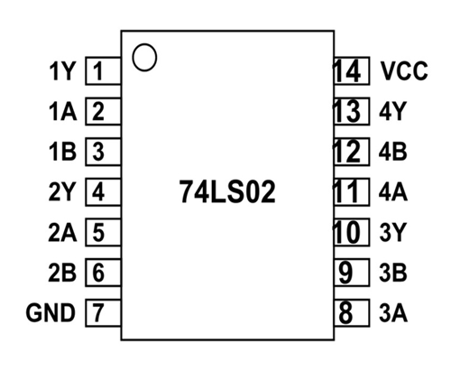
74LS02 Pinout, image source: components101.com

gBzQa41404304278, image source: elsalvadorla.org

c7f0549adca1460c8772518a902bf192, image source: www.robodocbd.com
Figure1, image source: www.cise.ufl.edu

1740_Logic%20Gates%20Homework%20Help%202, image source: www.tutorsglobe.com

EXNOR Gate Circuit Diagram, image source: circuitdigest.com

7486, image source: www.electronicshub.org

component mechanical logic gates spillerrecs den xor gate building rigginglogic thumbnail_relay logic_pin 85 on relay omron wiring diagram pcb circuit uses of 5v 12v output electri, image source: estrategys.co

truth%20table%20of%20ic7404, image source: www.zseries.in


nand, image source: elsalvadorla.org

Figure 1 Arduino Uno pin structure, image source: www.researchgate.net
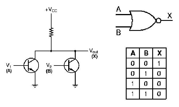
2 Input Transistor OR Gate, image source: elsalvadorla.org

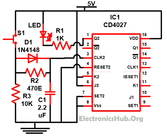
JK flip flop using CD4027, image source: www.electronicshub.org

paste_image31, image source: wiringdiagram.karaharmsphotography.com
4052, image source: www.elektropage.com

4029_pin, image source: www.elektropage.com


Comments
Post a Comment