18 Lovely At89C2051 Programmer Circuit Diagram
At89c2051 Programmer Circuit Diagram keil dd docs datashts atmel at89c2051 ds pdfAT89C2051 3 Pin Description VCC Supply voltage GND Ground Port 1 Port 1 is an 8 bit bi irectional I O port Port pins P1 2 to P1 7 provide internal pullups At89c2051 Programmer Circuit Diagram satsleuth Schematics aspxElectronic Circuit Schematics Note that all these links are external and we cannot provide support on the circuits or offer any guarantees to their accuracy
embedded lab blog heart rate measurement from fingertipCircuit Diagram The signal conditioning circuit consists of two identical active low pass filters with a cut off frequency of about 2 5 Hz This means the maximum measurable heart rate is about 150 bpm At89c2051 Programmer Circuit Diagram Intel MCS 51 commonly termed 8051 is a single chip microcontroller series developed by Intel in 1980 for use in embedded systems Intel s original versions were popular in the 1980s and early 1990s and enhanced binary compatible derivatives remain popular today It is an example of a complex instruction set computer and has microcontroller8051 Microcontroller Tutorial with Architecture The most commonly used set of microcontrollers belong to 8051 Family 8051 Microcontrollers continue to remain a preferred choice for a vast community of hobbyists and professionals
circuit zone catThis FM transmitter circuit is a quite fun project for electronics beginners so here s a circuit with the 2SC9018 transistor It uses the 2SC9018 high frequency transistor based on a different spin of the common base Collpit s oscillator At89c2051 Programmer Circuit Diagram microcontroller8051 Microcontroller Tutorial with Architecture The most commonly used set of microcontrollers belong to 8051 Family 8051 Microcontrollers continue to remain a preferred choice for a vast community of hobbyists and professionals cq cx ladder forum pl action viewallWhen compiling ANSIC with the yPlcCycleDuty checkbox ticked in Settings MCU Parameters no C code is generated for setting and
At89c2051 Programmer Circuit Diagram Gallery
electronic circuit schematics pic16f84 tone generator bit_photocell circuit diagram_fm transmitter diagram electrical house wiring pdf photocell block of signal generator actual, image source: farhek.com

lqv77_rt9241, image source: wiringdiagram.karaharmsphotography.com

aicp add on schematic, image source: www.pjrc.com
ISP89S_sch, image source: www.next.gr

generac transfer switch wiring diagram awesome generac power transfer switch wiring wiring diagrams of generac transfer switch wiring diagram, image source: wiringdiagram.karaharmsphotography.com


surround sound wiring diagram beautiful nice vm9311ts wiring diagram pinout s electrical circuit of surround sound wiring diagram, image source: wiringdiagram.karaharmsphotography.com
Hall Effect, image source: wiringdiagram.karaharmsphotography.com
Heart sound detection system structure diagram, image source: wiringdiagram.karaharmsphotography.com
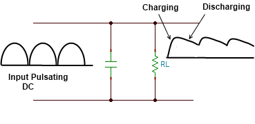
capacitor filter, image source: wiringdiagram.karaharmsphotography.com

ic 4049 clock pulse generator, image source: wiringdiagram.karaharmsphotography.com
intercom, image source: www.8051projects.info

avr_isp_sch, image source: www.electronicsteacher.com

schemat2, image source: drakeeng.tripod.com

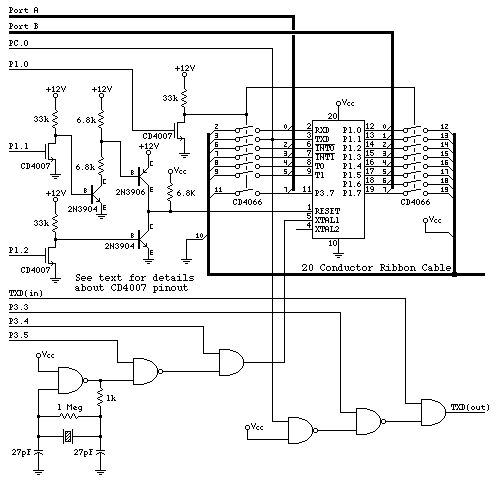
pg2051_1cct, image source: airborn.com.au

TP4056 Micro Charger Circuit 1 800x480 1 840x480, image source: wiringdiagram.karaharmsphotography.com

pl10455262 hf_fr4_multi_layered_pcb_circuit_boards_printed_circuit_board_manufacturing_process_1_5oz, image source: wiringdiagram.karaharmsphotography.com


Schematic illustration of techniques of genetic modication challenging the molecular, image source: wiringdiagram.karaharmsphotography.com


Comments
Post a Comment